(China (Mainland))

Product Summary
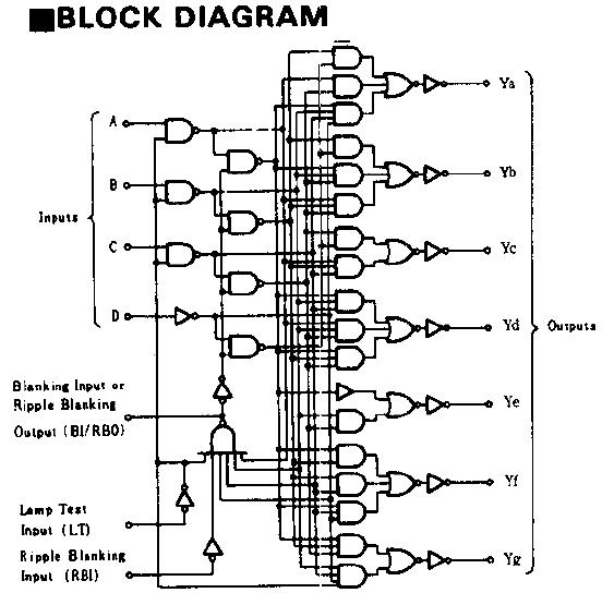
The HD74LS47P is a BCD-to-Seven Segment Decoder Driver. The HD74LS47P features active-low outputs designed for driving incandescent indicators directly. This, device has full rippfe-bfanking input/output controls and a lamp test input. Display patterns for BCD input counts above 9 are unique symbols to authenticate input conditions. This circuit incorporates automatic leading and/or taillingi-edge zero-btanking control (RBI and RBO). Lamp test (LT) of these types may be performed at any time when the BI/RBO node is at a high level. It contains an overriding blanking input (Bl) which can be used to control the lamp intensity of pulsing or to inhibit the outputs. Inputs and outputs are entirely compatible for use with TTL or DTL logic outputs.
Parametrics
HD74LS47P absolute maximum ratings: (1)Supply voltage, Vcc: 7.0V; (2)Input voltage, VtN: 7.0V; (3)Output current, lO: 200mA; (4)Output current (off-state), Io(off): 1mA; (5)Operating iemperature range, Tapr: -20 to + 75℃; (6)Storage temperature range, Tstg: -65 to +150℃.
Features
HD74LS47P features: (1)Supply voltage, Vcc: 4.75 to 5.25V; (2)Off state output voltage, VO(off): 15V; (3)On state output current, IO: 24mA; (4)High level output current, ION: -50μA; (5)Low level output current, IOI: 3.2mA; (6)Operating temperature range, Topt: -20 to 75℃.
Diagrams
 |
 HD7425FPA |
Other |
|
Data Sheet |
Negotiable |
|
||||
|
HD74AC |
Other |
|
Data Sheet |
Negotiable |
|
||||
|
HD74AC00 |
Other |
|
Data Sheet |
Negotiable |
|
||||
|
HD74AC02 |
Other |
|
Data Sheet |
Negotiable |
|
||||
|
HD74AC04 |
Other |
|
Data Sheet |
Negotiable |
|
||||
|
HD74AC04FP-EL |
Other |
|
Data Sheet |
Negotiable |
|
||||