(China (Mainland))


Product Summary
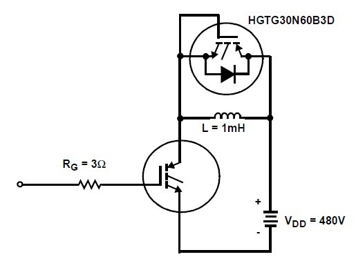
The G30N60B3 is a MOS gated high voltage switching device combining the best features of MOSFETs and bipolar transistors. This G30N60B3 has the high input impedance of a MOSFET and the low on-state conduction loss of a bipolar transistor. The much lower on-state voltage drop varies only moderately between 25oC and 150oC. The IGBT used is the development type TA49170. The diode used in anti-parallel with the G30N60B3 is the development type TA49053.
Parametrics
G30N60B3 absolute maximum ratings: (1)60A, 600V, TC = 25oC; (2)600V Switching SOA Capability; (3)Typical Fall Time: 90ns at TJ = 150oC; (4)Short Circuit Rating; (5)Low Conduction Loss; (6)Hyperfast Anti-Parallel Diode.
Features
G30N60B3 features: (1)Collector to Emitter Voltage: BVCES 600 V; (2)Collector Current Continuous, At TC = 25℃, IC25: 60 A; At TC = 110℃, IC110: 30 A; (3)Average Diode Forward Current at 110℃, IEC(AVG): 25 A; (4)Collector Current Pulsed, ICM: 220 A; (5)Gate to Emitter Voltage Continuous, VGES: ±20 V; (6)Gate to Emitter Voltage Pulsed, VGEM: ±30 V; (7)Switching Safe Operating Area at TJ = 150℃, SSOA: 60A at 600V; (8)Power Dissipation Total at TC = 25℃, PD: 208 W; (9)Power Dissipation Derating TC > 25℃: 1.67 W/℃; (10)Operating and Storage Junction Temperature Range, TJ, TSTG: -55 to 150 ℃; (11)Maximum Lead Temperature for Soldering, TL: 260 ℃; (12)Short Circuit Withstand Time (Note 2) at VGE = 12V, tSC: 4 μs; (13)Short Circuit Withstand Time (Note 2) at VGE = 10V, tSC: 10 μs.
Diagrams