(China (Mainland))

Product Summary
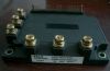
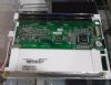
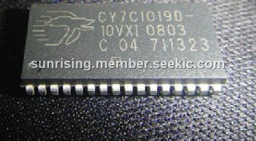
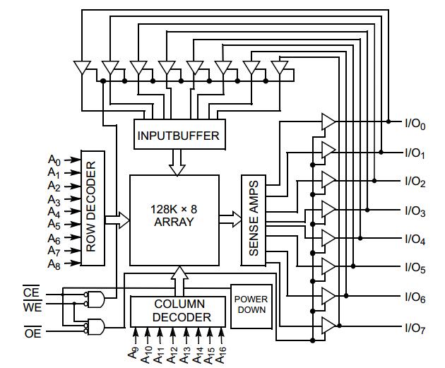
The CY7C1019DV33-10VXI is a high-performance CMOS static RAM organized as 131,072 words by 8 bits. Easy memory expansion is provided by an active LOW Chip Enable (CE), an active LOW Output Enable (OE), and three-state drivers. The CY7C1019DV33-10VXI has an automatic power-down feature that significantly reduces power consumption when deselected. Writing to the device is accomplished by taking Chip Enable (CE) and Write Enable (WE) inputs LOW. Data on the eight I/O pins (I/O0through I/O7) is then written into the location specified on the address pins (A0 through A16).
Parametrics
CY7C1019DV33-10VXI absolute maximum ratings: (1)Storage Temperature: -65℃ to +150℃; (2)Ambient Temperature with Power Applied: -55℃ to +125℃; (3)Supply Voltage on VCCto Relative GND: -0.3V to + 4.6V; (4)DC Voltage Applied to Outputs in High-Z State: -0.3V to VCC+ 0.3V DC Input Voltage: -0.3V to VCC+ 0.3V; (5)Current into Outputs (LOW): 20 mA; (6)Static Discharge Voltage: > 2001V; (7)(per MIL-STD-883, Method 3015) Latch-up Current: > 200 mA.
Features
CY7C1019DV33-10VXI features: (1)Pin- and function-compatible with CY7C1019CV33; (2)High speed,tAA= 10 ns; (3)Low Active Power, ICC= 60 mA @ 10 ns; (4)Low CMOS Standby Power, ISB2= 3 mA; (5)2.0V Data retention; (6)Automatic power-down when deselected; (7)CMOS for optimum speed/power; (8)Center power/ground pinout; (9)Easy memory expansion with CE and OE options; (10)Available in Pb-free 32-pin 400-Mil wide Molded SOJ, 32-pin TSOP II and 48-ball VFBGA packages.
Diagrams
| Image | Part No | Mfg | Description |  |
Pricing (USD) |
Quantity | ||||||||||||
|---|---|---|---|---|---|---|---|---|---|---|---|---|---|---|---|---|---|---|
 |
 CY7C1019DV33-10VXI |
Cypress Semiconductor |
SRAM 1M 512K IND FAST ASYNC SRAM |
Data Sheet |
|
|
||||||||||||
|
CY7C1019DV33-10VXIT |
Cypress Semiconductor |
SRAM 1M 512K IND FAST ASYNC SRAM |
Data Sheet |
|
|
||||||||||||